Add AND9137_SO-3-8_EP_5x6mm_P1.27mm footprint
Ref https://github.com/KiCad/kicad-footprints/issues/1000
Datasheet: https://www.onsemi.com/pub/Collateral/AND9137-D.PDF
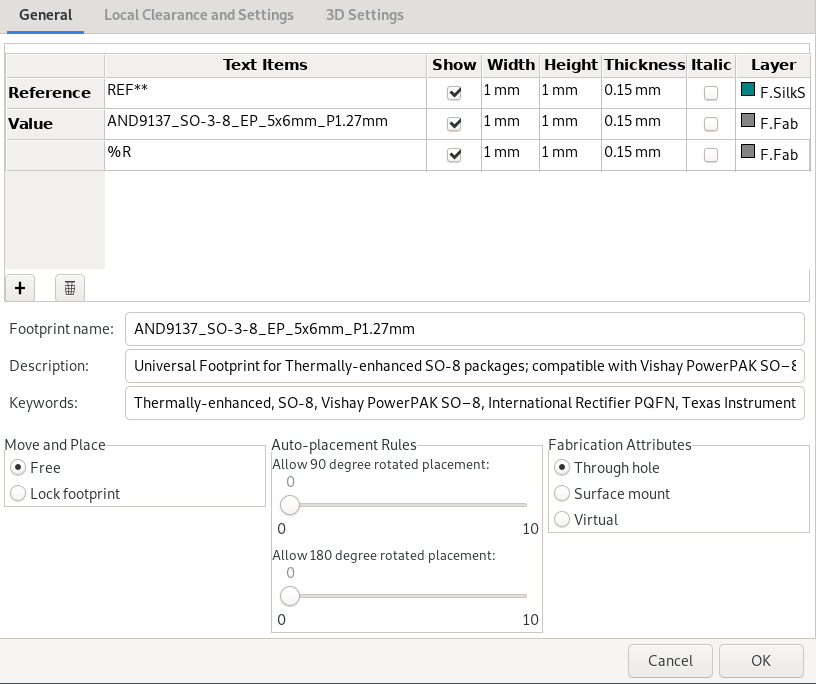


3d is already-existing ${KISYS3DMOD}/Package_SO.3dshapes/Vishay_PowerPAK_SO-8.wrl, which this footprint is specifically designed for.
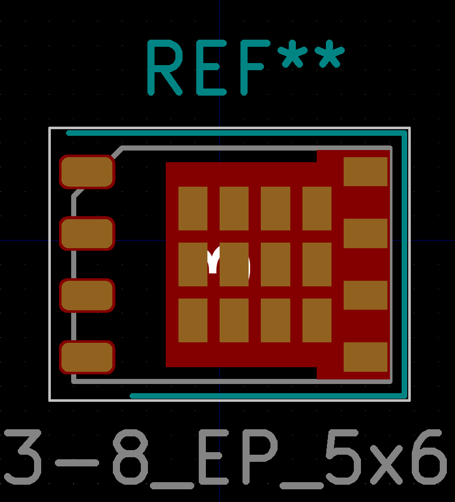
This footprint almost exactly implements the footprint described in AND9137; the only difference is that this footprint has a .175mm radius on the top 4 pins because some guy on stackexchange suggested it's a good idea.
Another point of note is the pin numbering. Instead of numbering this as 1-8, I've numbered it 1-3. All packages that this claims compatibility for have source=1-3, gate=4, and drain=5-8. If you'd like to confirm compatibility yourself, here are the datasheets:
- http://www.farnell.com/datasheets/1704644.pdf
- http://www.vishay.com/docs/62839/si7149adp.pdf
- https://www.infineon.com/dgdl/irfhm9331pbf.pdf?fileId=5546d462533600a4015356237f7e1f59
- https://www.ti.com/lit/ds/symlink/csd18537nq5a.pdf
- http://aosmd.com/res/data_sheets/AON6236.pdf
- https://www.st.com/content/ccc/resource/technical/document/datasheet/d7/9b/35/84/f3/31/44/19/DM00098815.pdf/files/DM00098815.pdf/jcr:content/translations/en.DM00098815.pdf
- https://www.infineon.com/dgdl/DS_BSC014N04LS_2_1.PDF?folderId=db3a304313b8b5a60113cee8763b02d7&fileId=db3a3043353fdc16013552e99a8147f1
- https://assets.nexperia.com/documents/data-sheet/PSMN030-60YS.pdf
- https://www.renesas.com/us/en/doc/products/transistor/002/r07ds0765ej0200_rjk03m1dpa.pdf
- https://www.onsemi.com/pub/Collateral/FDMS86202-D.pdf
- https://toshiba.semicon-storage.com/info/docget.jsp?did=15504&prodName=TPW4R50ANH
- http://www.magnachip.com/powersolutions/down.php?filename=MDU3605.pdf
- https://www.rohm.com/datasheet/RS1E130GN/rs1e130gntb-e
- http://www.1mos.com/upload/file/UBIQ/QM4006M6.pdf
- https://datasheet.lcsc.com/szlcsc/1904151131_NIKO-Semicon-PKCH2BB_C384597.pdf
- https://datasheet.octopart.com/UPA2724UT1A-E1-AZ-NEC-datasheet-166712.pdf
Labeling the pins like this makes it possible to use the generic mosfet symbols in schematics.
The library conventions were carefully read and followed.
All contributions to the kicad library must follow the KiCad library convention
Thanks for creating a pull request to contribute to the KiCad libraries! To speed up integration of your PR, please check the following items:
-
Provide a URL to a datasheet for the footprint(s) you are contributing -
An example screenshot image is very helpful -
If there are matching symbol or 3D model pull requests, provide link(s) as appropriate -
Check the output of the Travis automated check scripts - fix any errors as required -
Give a reason behind any intentional library convention rule violation.